Directional Solvent Vapour Annealing Process Optimization
Introduction:
There is an escalating electronic waste crisis fueled by the short lifespan of conventional electronic products and the need for sustainable and eco-friendly alternatives has over the years become extremely crucial. Organic electronics is a class of electronics that mostly comprise of materials that organic in nature as they provide several benefits in terms of being eco-friendly and non-toxic in terms of human interactions. They present characteristics such as flexibility, low cost, and scalability.
This project embarks on the optimization of fabrication processes for Organic Field-Effect Transistors (OFETs). Major objectives of the project include improving electrical performance of the OFETs by varying pre-decided factors that may affect the performance. Further integrate nature-oriented materials and biodegradability.
This project undertakes a parameter optimization study on a previous paper introducing a novel techniques for creating crystals with certain alignment using Directional Solvent Vapor Annealing(DSVA). In DSVA for crystal alignment in solution-processed organic semiconductors is proposed. The drop-cast technique is enhanced using this postprocessing scheme of the solvent vapor annealing with additional alignment of the crystals.
Organic Field Effect Transistors
Structures
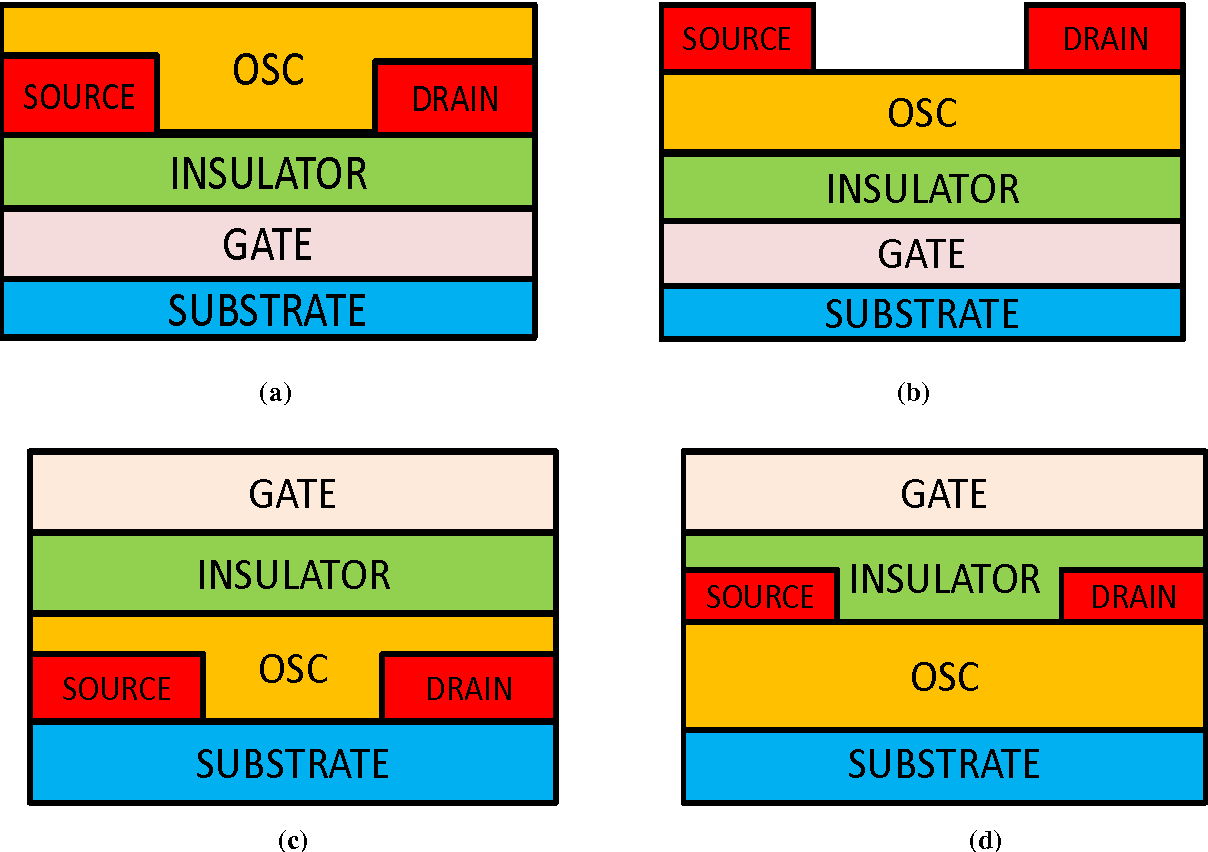
Organic thin film transistors (OTFTs) are active electronic components that can be printed and used in analog, digital, and mixed-signal circuits. They can also be used as stand-alone sensors where the change in electrical current can be mapped to the physical change being sensed . OTFTs are composed of three main components: contacts (source (S), drain (D), and gate (G)), a dielectric thin film, and an organic semiconducting thin film (OSC). Contacts are typically made of silver, gold, copper, or ITO. However, there are no standards or trends for dielectrics or organic semiconducting material due to the many options and combinations available. The components of an OTFT can be ordered into four different structures: Bottom Gate Top Contact (BGTC), Bottom Gate Bottom Contact (BGBC), Top Gate Bottom Contact (TGBC), and Top Gate Top Contact (TGTC). Both BGTC and TGBC are considered staggered transistors due to their structure, while BGBC and TGTC are considered coplanar transistors for the same reason . Figure 1 shows the four different structures of OTFTs.
Operating Principles
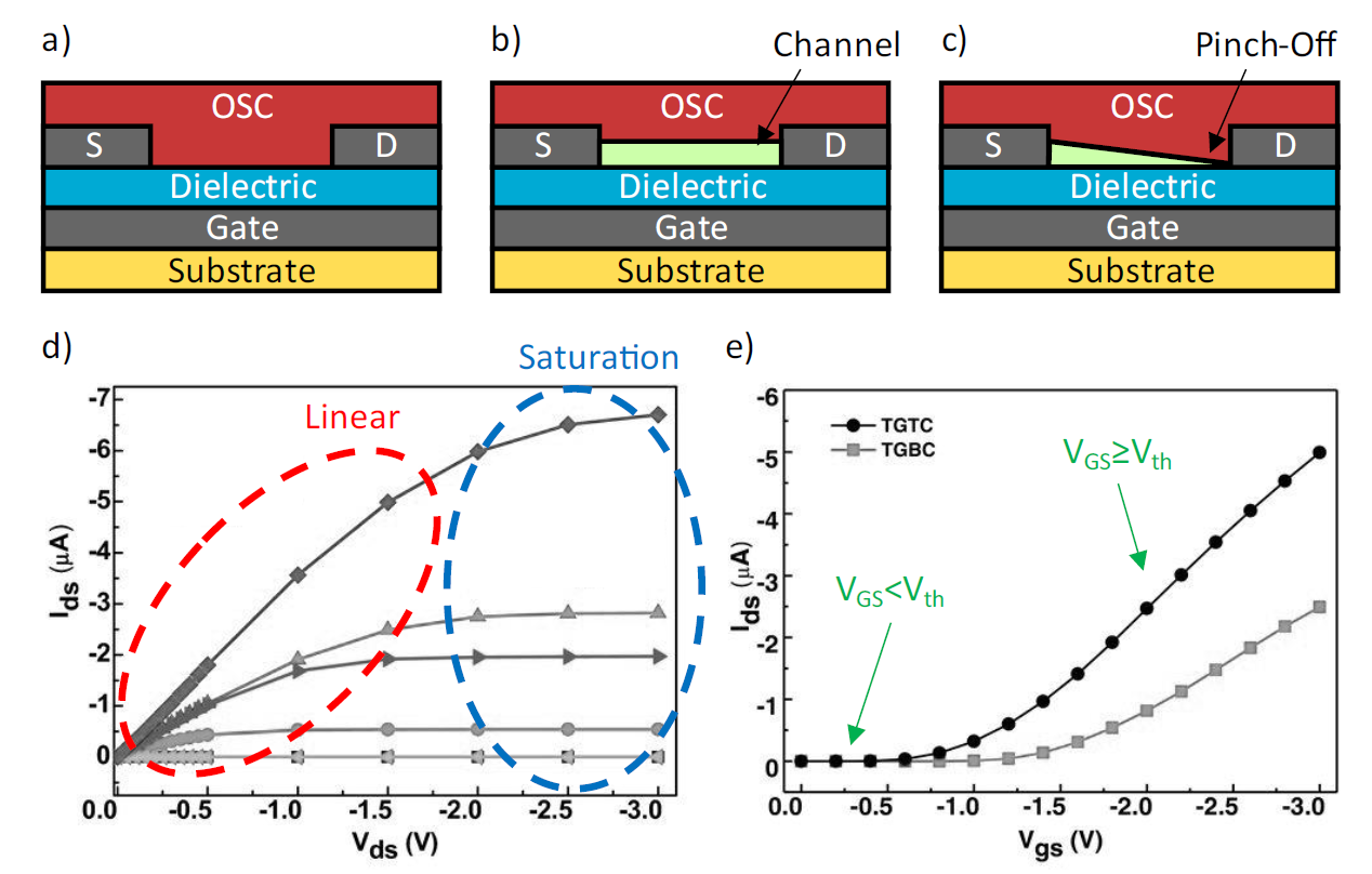
In both Organic thin-film transistors(OTFTs) and traditional silicon metal-oxide semiconductor field0effect transistors(MOSFETs), the operating principles share similarities. OTFTs the same as MOSFETs involve source and drain electrodes directly contacting the semiconductor with the gate contact insulated from the the semiconductor by a dielectric film. Applying a voltage bias between the gate and source electrodes (VGS) leads to carrier accumulation near the semiconductor-dielectric interface, creating a channel for current flow when a voltage bias is applied between the drain and source (VDS). The minimum VGS required for channel creation is called the threshold voltage (Vth).
The primary difference between OTFTs and MOSFETs lies in the channel formation process. MOSFETs undergo an inversion process, resulting in charge carriers in the channel opposite to those in the semiconductor bulk. In OTFTs, the charge carriers in the channel are same as those in the organic semiconductor (OSC) bulk.
Despite the differences in the type of charge transport in organic
and inorganic semiconductors, OTFTs exhibit similar regions of
operation to MOSFETs, including cut-off, linear, and saturation.
When
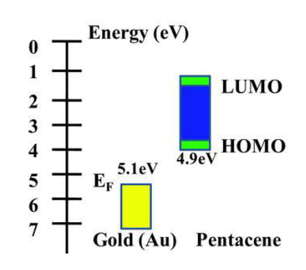
The fundamental operation of an OTFT involves utilizing the
capacitor principle, generating an electric field in the dielectric
in response to a gate-source voltage (
Characteristics:
Several key parameters determine the performance of an organic
transistor, and these include field-dependent mobility (
-
Mobility (
-
Threshold Voltage (
-
On/Off Current Ratio (
-
Sub-threshold Slope (SS): Sub-threshold slope (SS) gauges the change in drain current on a logarithmic scale concerning the change in gate biasing. It reflects impurity concentration, interface state, and trap density, influencing the switching behavior of a transistor. SS is a crucial parameter for evaluating the efficiency of a transistor as a switch, determined by the ratio of the change in gate biasing to the change in drain current on a logarithmic scale. It plays a key role in determining the device’s suitability for various applications.
Directional Solvent Vapor Annealing (DSVA)
Experimental Setup
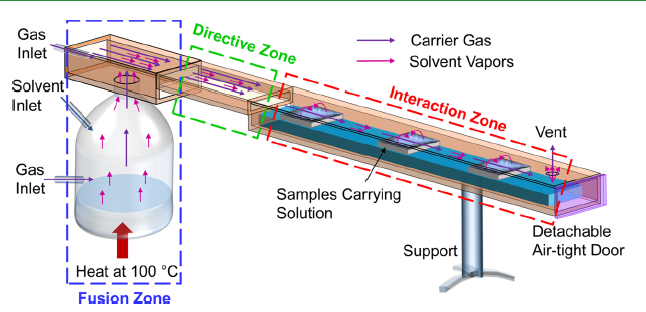
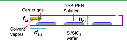
The DSVA setup was specially designed and built to perform both deposition and postprocessing. The schematic diagram in Figure 4 illustrates the setup, comprising three zones: fusion, directive, and interaction. The fusion zone features a glass vessel filled with a solvent at the bottom, heated by a hot plate. The vessel has two inlets for solvent and carrier gas. At the top of the fusion zone, there is a chamber with an inlet for pushing the gas-vapor mixture into the directive zone. This is where the solvent vapor is generated, mixed with the carrier gas, and propelled into the directive zone.
The directive zone is a hollow rectangular chamber with very low
height, providing high directionality to the gas-vapor mixture. The
mixture flows continuously from the fusion zone to the interaction
zone. In the interaction zone, there is a long and narrow tube with
a stage that can be adjusted to place the samples at different
positions. The interaction between the gas-vapor mixture and the
substrate with the solution takes place in this zone. The tube has a
removable door at the end for inserting or removing samples, and a
small vent at the top for gas discharge. Figure 5 presents the
cross-sectional view of the tube, indicating different parameters.
Comparison of Various Solution-Processing Techniques
Table shown in Figure 6
Here is the table rewritten in the requested format:Conclusions of the Initial Study
DSVA is a proposed solution processing technique for organic semiconductors that combines SVA and gas flow. DSVA improves the molecular self-assembly and alignment of the semiconductor films by using SVA and gas−vapor mixture, respectively. The degree of crystallinity and alignment of the semiconducting ribbons depends on the flow rate of the carrier gas and the position of the substrate in the interaction tube. The optimal conditions for DSVA produce a semiconducting layer with well-aligned and interconnected ribbons. Such a layer leads to a high performance of the OFETs, suggesting that DSVA is a versatile technique for solution processing of organic semiconductors.
Background and Problem Statement
Problem Statement
The escalating global issue of electronic waste demands a shift towards sustainable alternatives. While high performance organic electronics particularly Organic Field-Effect Transistors(OFETs) show promise, their performance is still not at par with traditional inorganic electronics. The task that needs to be undertaken is that we need to seamlessly integrate high performance and eco-friendliness while navigating through complex procedures such as material selection and fabrication processes and produce OFETs that are air-stable and biodegradable in nature.
One Technique that is used to create OFETs is drop casting the organic semiconductor on your substrates however even though this technique has shown promise but this technique doesn’t take into account the need for alignment of crystals or the elongation of crystals. Hence another novel technique can be used post drop-casting that uses Directional Solvent Vapor Annealing or DSVA. However, since DSVA is a novel technique and there is lack of research on several parameters that may or may not affect the techniques’ outcomes. So, there is a need for a parameter optimization study that varies several relevant parameters and reports the outcomes.
Background
Organic semiconductor solution-processing methods are gaining attention for their cheaper production costs and eco-friendly nature, aiming to compete with complex vacuum processing techniques. Factors influencing the performance of solution-processed devices include crystallinity, molecular packing, morphology, and orientation of crystalline domains. The main challenge in solution-processed semiconductors arises from three-dimensional crystal growth, leading to inconsistent charge transport and device behavior.
Common methods like drop casting and spin coating present a trade-off between molecular settlement time and crystallinity, impacting uniformity and consistency in device performance. Alternative processing and post-processing methods, such as zone casting, dip coating, and inkjet printing, have been explored to control molecular self-assembly and enhance crystalline order. Incorporating post-processing methods like solvent vapor annealing (SVA) has proven advantageous for improving self-organization and crystalline order in semiconductor films.
The proposed directional solvent vapor annealing (DSVA) integrates deposition and post-processing, aiming to achieve highly aligned and crystalline films for high-performance organic semiconductor devices. DSVA involves the flow of a carrier gas and solvent vapors in a specific direction and proximity to the substrate, promoting macroscopic alignment and microscopic molecular self-assembly in crystalline domains.
Parameters like carrier gas flow rate, substrate proximity, and
position in the interaction tube critically affect overall
crystallinity, alignment, and device performance. DSVA application
in organic field-effect transistors (OFETs) fabrication demonstrated
a maximum mobility of
Work done, Results and Discussions
Work Done
Experimental Setup
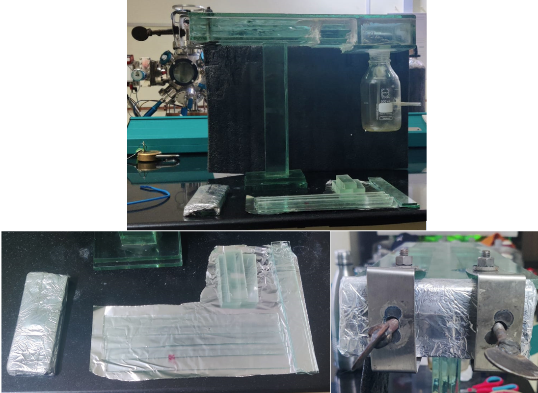
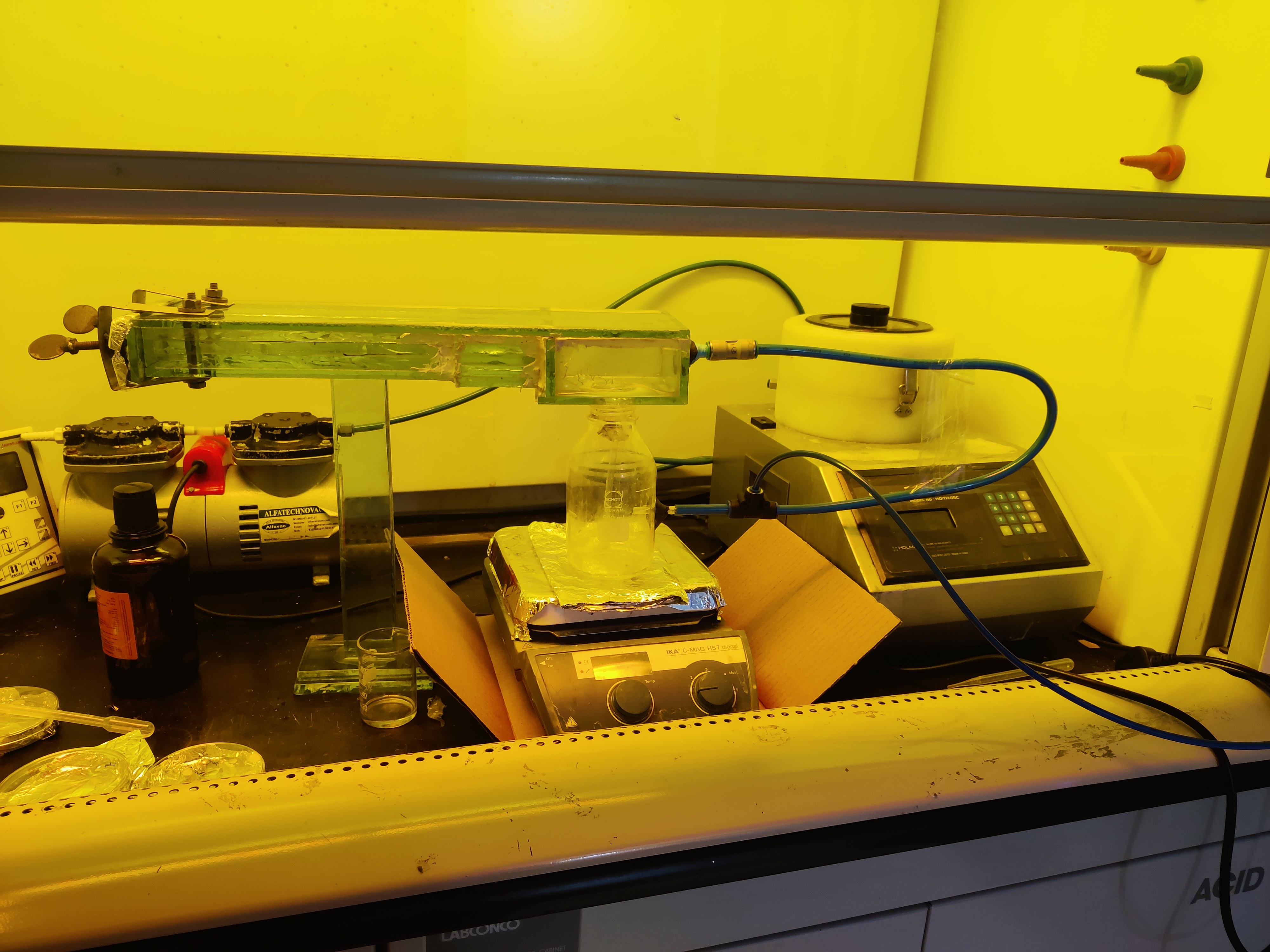
The experimental setup was in dysfunctional state at the start of the project and hence required tune-up and testing for any malfunction that may have been caused due to the apparatus being unused for a long time.
Finally, There were some issues regarding the cleaning of the apparatus as the glass vessel that rests on a hot plate has no big enough opening for a proper cleaning and the adhesive did not interact well with Iso-propyl alcohol and seem to disintegrate on contact. So another way was employed as toluene was used under a fume hood and then heated and vapours were allowed to flow from inside the glass vessel to the rest of the apparatus hence cleaning the entire apparatus. These are pictures of the final apparatus.
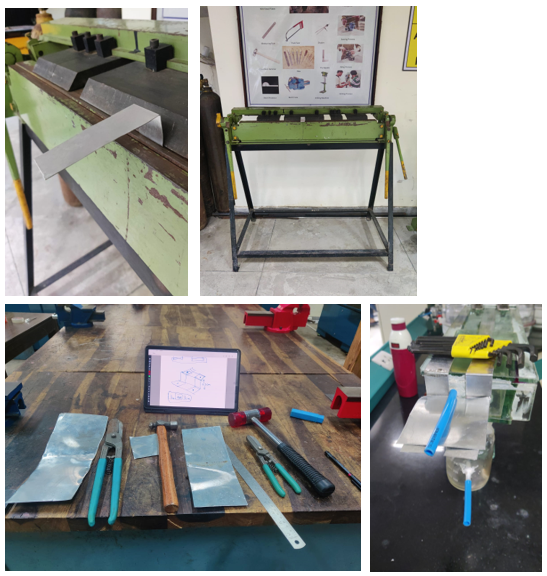
Metal Bracket
A metal Bracket was required to handle the weight of the gas pipe that was bringing the end of the apparatus down and straining the glass pipes directly glued to the apparatus.
Finalization of Parameters
A lot of parameters were discussed and pondered upon, finally coming up with a list of parameters that will be used in the parameter optimization study. The following parameters will be used:
-
Height of the tube ceiling with respect to the floor of the stage
-
Distance of the midpoint of the sample from the beginning of the interaction tube
Flow rate of the carrier gas
-
Concentration of the gas-vapor mixture in different regions of the interaction tube
Incline of the sample
Substrate material
Mixing ratio
Some Preliminary Experiments
There were some basic questions that arose during the project and some basic preliminary experiments without much experimental setup were designed to answer those questions.
There was one experiment where 2 samples of ITO-PET substrate were taken after proper cleaning process and then through Atomic Layer Deposition (ALD) Hafnium was deposited on only one of them and then 6,13-Bis(triisopropylsilylethynyl)pentacene also known as TIPS-Pentacene was drop-casted on both those samples.
Then to simulate something like DSVA, Nitrogen gas was passed over the samples and to prevent direct flow of the gas over the samples a simple cardboard piece was placed. The inferences from the experiment included that the only the flow of gas without solvent vapors was not responsible for the crystal formation and Hafnium provided better crystallinity as compared to sample without Hafnium.
Another Experiment was conducted and this experiment included two samples based on ITO-PET and one was coated Polystyrene(PS) and then TIPS-Pentacene was drop casted on it. And another sample which was drop-casted with a pre mixed TIPS-Pentacene and Polystyrene solution in Toluene. The sample that was coated with Polystyrene and then TIPS-Pentacene showed better crystallinity however the electrical characteristics were not tested. In an ideal scenario the TIPS-Pentacene and PS mix should have shown phase separation during crystal formation.
Experiment Design and Experiment
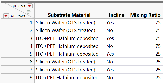
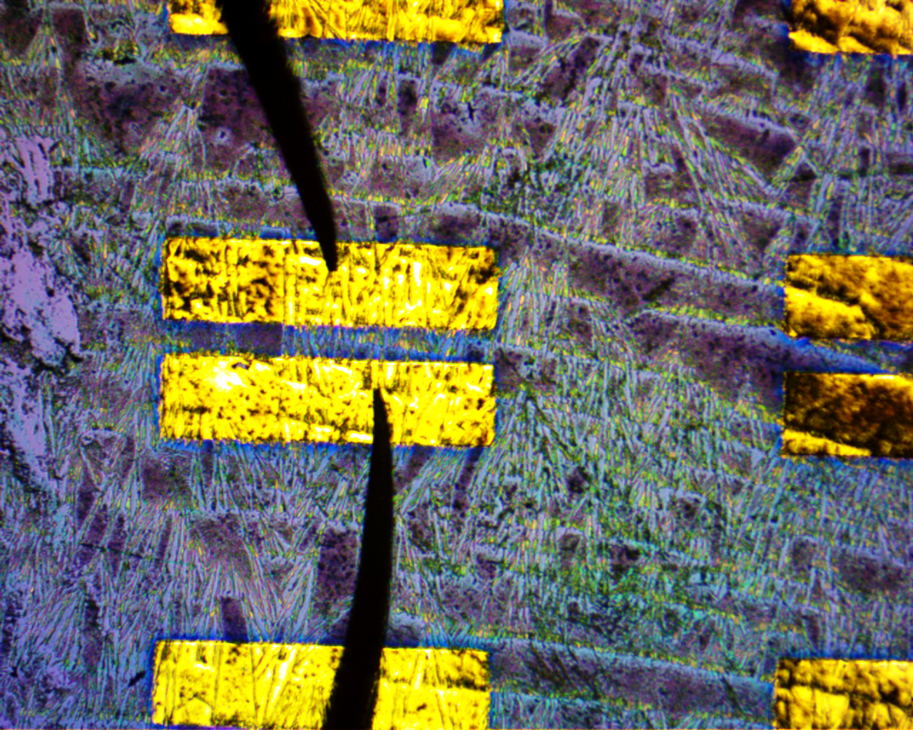
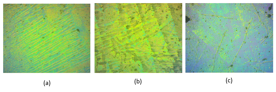
As Part of the Preliminary experimental design prior to a full factorial Design of Experiments method to find out factors that seem to make a difference for our process. Several Factors like Mixing Ratio,Substrate Material,Incline of the sample were varied and then the experiment was run as described above with bare minimum air flow and Toluene as Solvent heated to 120 °C inside the fume hood. The experiment was run Thrice for an hour each time and the film formed was observed under a microscope. Since it is already known to us height of tube ceiling with respect to the floor of the stage,Distance of the midpoint of the sample from the beginning of the interaction tube, Flow rate of the carrier gas have effect on the film of the sample so these were made constant at 6 mm , (1.5 inches,4 inches, 6 inches), 0.5L/min.
Substrate Preparation
Two types of substrates were used in the experiment ITO-PET and Silicon Wafer. Both of them were cleaned using Iso-propyl Alcohol,Acetone and Distilled Water. After which ITO-PET had a deposition of Hafnium using Atomic Layer Deposition and Silicon Wafer was submerged in 5 mM Octadecyltrichlorosilane(OTS) in Toluene for 24 hours.
Solution Preparation
A 0.5 wt% solution of TIPS-pentacene in toluene (5 mg/mL) was prepared by stirring for 3 h at 65 °C. Along with 0.5 wt% solution of Polystyrene in Toluene (5 mg/ml) in a similar manner. The were mixed in various ratios such 100% (Pure TIPS-Pentacene) , 25% and 75% .
Experiment
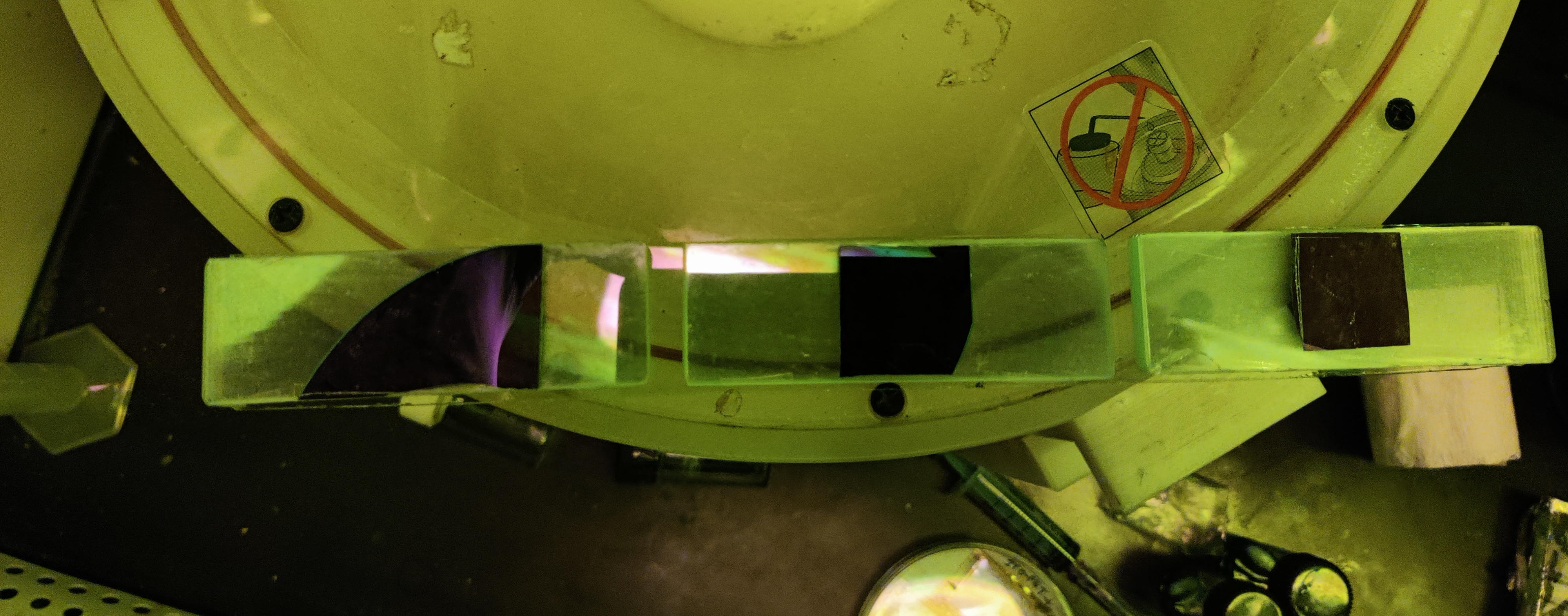
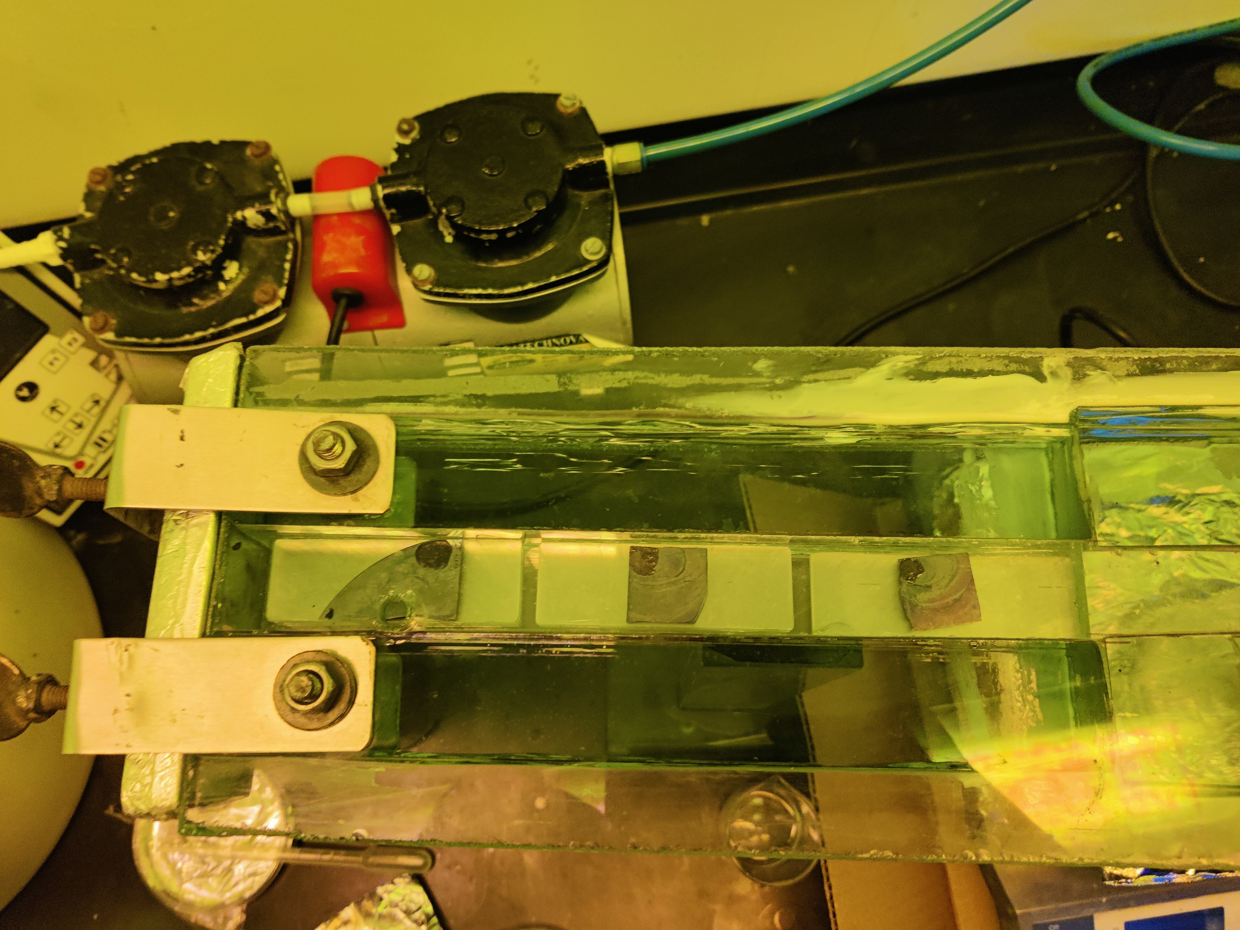
The prepared solutions were drop casted on the samples according to a prior experimental design mapping various combination to make it easy to identify factor contributions.Then Nitrogen was run through the apparatus.
Source-Drain Deposition
Characterization
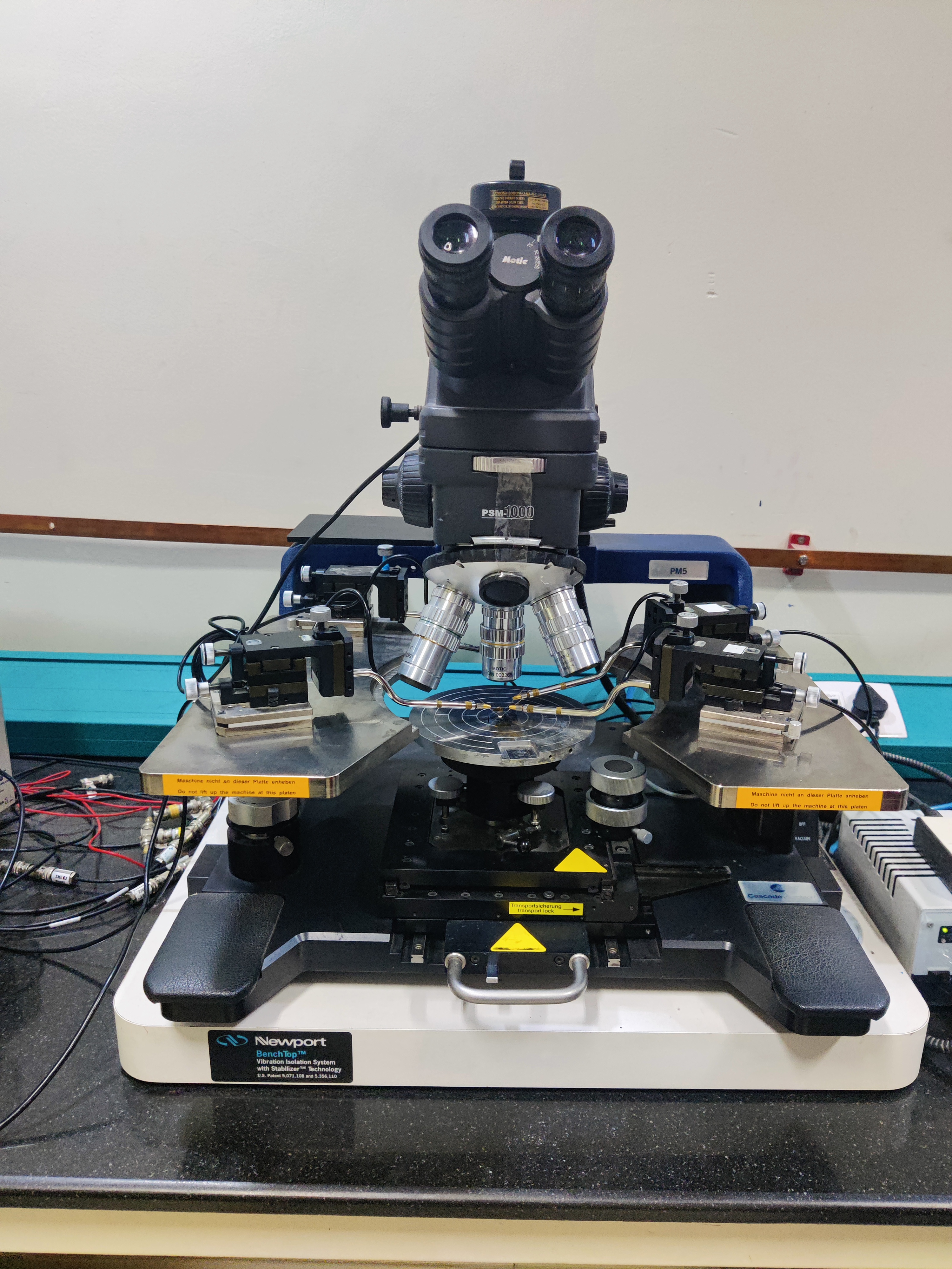
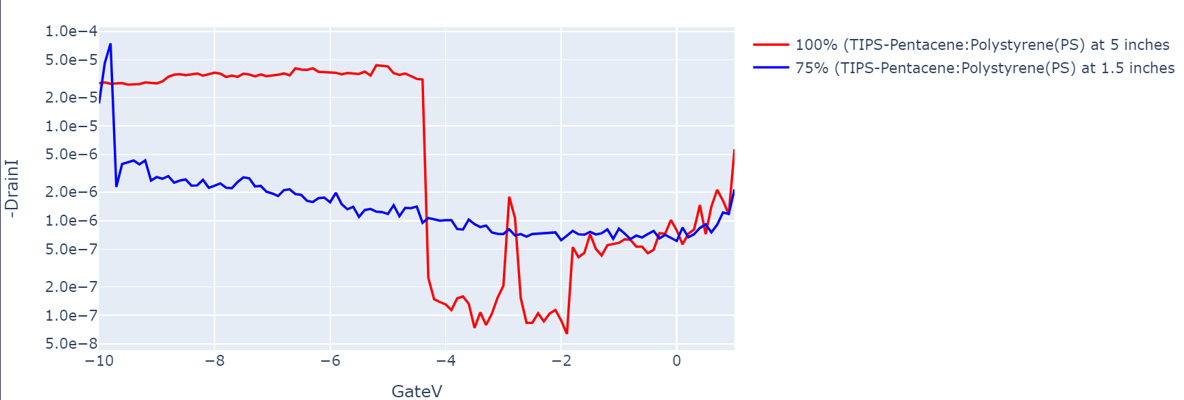
Electrical Characterization was done on the samples using a Probe Station. And relevant data was extracted showcasing the samples’ input output characteristics in various Regions of Operation.
Results and Observations
Film Images
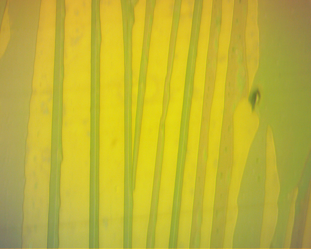
Figures 15-17

Plots
Figures 18-21

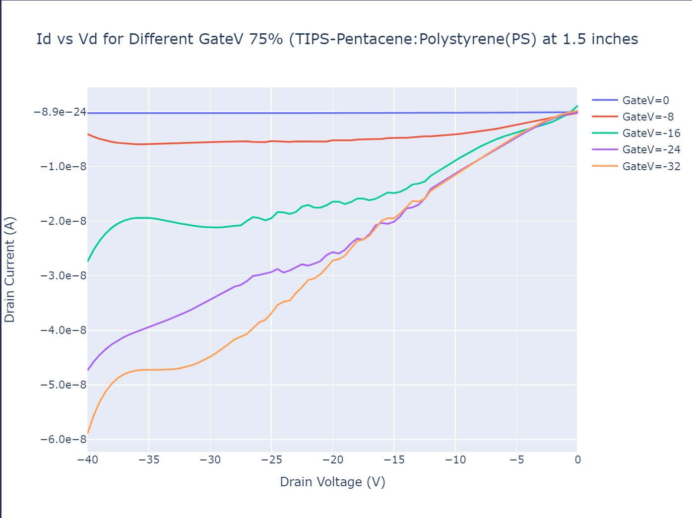
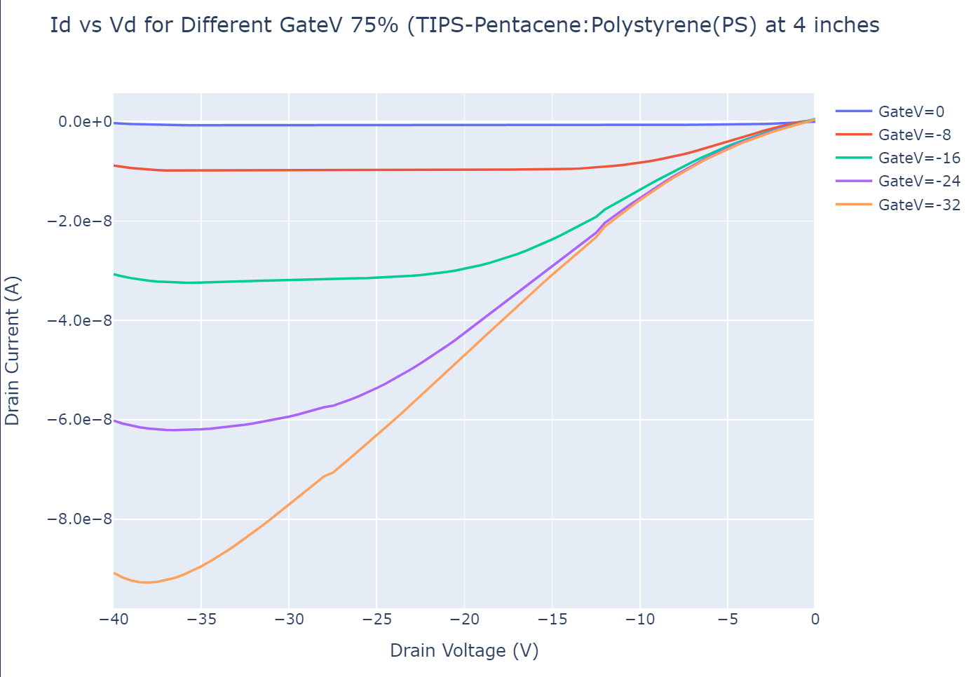
Conclusions
-
The substrate ITO-PET isn’t hydrophilic enough to hold our solution in a stable form in front of the Nitrogen gas. So, some more surface treatment needs to be done to the ITO-PET for better attraction towards the solution.The non-uniform film cause short circuits.
-
The Factor Mixing Ratio has an effect on the quality of the film higher concentration provided better quality film with uniform crystals and in the end relatively better performance.
-
The Factor Incline didn’t have a positive effect instead resulted in accumulation of the solution at the bottom end not being able to form a film on the the sample apart from the very bottom
-
The Factor Substrate Material Does have an effect as the interactions with solution and hydrophobicity of every substrate is different and surface treatments also make a difference.
-
In respect to prior testing with the apparatus in the original paper we know that height of tube ceiling with respect to the floor of the stage,Distance of the midpoint of the sample from the beginning of the interaction tube, Flow rate of the carrier gas,
Future Work
-
Designing and Completion of a Full Factorial Design of Experiments
-
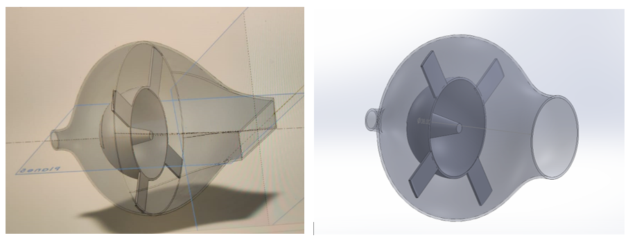
Designing an entirely new DSVA apparatus with better flow and interaction with solvent in a better manner
References
-
Bharti, D. & Tiwari, S. P. (2016). Crystallinity and Performance Improvement in Solution Processed Organic Field-Effect Transistors Due to Structural Dissimilarity of the Additive Solvent. Synth. Met., 215, 1-6.
-
Reig, M., Puigdollers, J., & Velasco, D. (2015). Molecular Order of Air-Stable p-type Organic Thin-Film Transistors by Tuning the Extension of the π-Conjugated Core: The Cases of Indolo[3,2-B]Carbazole and Triindole Semiconductors. J. Mater. Chem. C, 3, 506-513.
-
Kalita, A., Subbarao, N. V. V., & Iyer, P. K. (2015). Large-Scale Molecular Packing and Morphology-Dependent High Performance Organic Field-Effect Transistor by Symmetrical Naphthalene Diimide Appended with Methyl Cyclohexane. J. Phys. Chem. C, 119, 12772-12779.
-
Kim, M. J., Heo, H. W., Suh, Y. K., & Song, C. K. (2011). Morphology Control of TIPS-Pentacene Grains with Inert Gas Injection and Effects on the Performance of OTFTS. Org. Electron., 12, 1170-1176.
-
Shao, W., Dong, H., Jiang, L., & Hu, W. (2011). Morphology Control for High Performance Organic Thin Film Transistors. Chem. Sci., 2, 590-600.
-
He, Z., Chen, J., Sun, Z., Szulczewski, G., & Li, D. (2012). Air-Flow Navigated Crystal Growth for TIPS Pentacene-Based Organic Thin-Film Transistors. Org. Electron., 13, 1819-1826.
-
Kumatani, A., Liu, C., Li, Y., Darmawan, P., Takimiya, K., Minari, T., & Tsukagoshi, K. (2012). Solution-processed, Self-organized Organic Single Crystal Arrays with Controlled Crystal Orientation. Sci. Rep., 2(393).
-
Jeong, H., Han, S., Baek, S., Kim, S. H., & Lee, H. S. (2016). Dense Assembly of Soluble Acene Crystal Ribbons and Its Application to Organic Transistors. ACS Appl. Mater. Interfaces, 8, 24753-24760.
-
Wu, K.-Y., Hsieh, C.-T., Wang, L.-H., Hsu, C.-H., Chang, S.-T., Lan, S.-T., Huang, Y.-F., Chen, Y.-M., & Wang, C.-L. (2016). Influences of Out-Of-Plane Lattice Alignment on the OFET Performance of TIPS-PEN Crystal Arrays. Cryst. Growth Des., 16, 6160-6166.
-
He, T., Zhang, X., Jia, J., Li, Y., & Tao, X. (2012). Three-Dimensional Charge Transport in Organic Semiconductor Single Crystals. Adv. Mater., 24, 2171-2175.
-
Chen, J., Tee, C. K., Shtein, M., Martin, D. C., & Anthony, J. (2009). Controlled Solution Deposition and Systematic Study of Charge-Transport Anisotropy in Single Crystal and Single-Crystal Textured Tips Pentacene Thin Films. Org. Electron., 10, 696-703.
-
Headrick, R. L., Wo, S., Sansoz, F., & Anthony, J. E. (2008). Anisotropic Mobility in Large Grain Size Solution Processed Organic Semiconductor Thin Films. Appl. Phys. Lett., 92(063302).
-
Kim, C. S., Lee, S., Gomez, E. D., Anthony, J. E., & Loo, Y.-L. (2008). Solvent-Dependent Electrical Characteristics and Stability of Organic Thin-Film Transistors with Drop Cast bis(triisopropylsilylethynyl) Pentacene. Appl. Phys. Lett., 93(103302).
-
Park, S. K., Mourey, D. A., Han, J.-I., Anthony, J. E., & Jackson, T. N. (2009). Environmental and Operational Stability of Solution-Processed 6,13-bis(triisopropyl-silylethynyl) Pentacene Thin Film Transistors. Org. Electron., 10, 486-490.
-
Choi, D., Ahn, B., Kim, S. H., Hong, K., Ree, M., & Park, C. E. (2012). High-Performance Triisopropylsilylethynyl Pentacene Transistors via Spin Coating with a Crystallization-Assisting Layer. ACS Appl. Mater. Interfaces, 4, 117-122.
-
Park, S. K., Jackson, T. N., Anthony, J. E., & Mourey, D. A. (2007). High Mobility Solution Processed 6,13-bis(triisopropyl-silylethynyl) Pentacene Organic Thin Film Transistors. Appl. Phys. Lett., 91(063514).
-
He, Z., Xiao, K., Durant, W., Hensley, D. K., Anthony, J. E., Hong, K., Kilbey, S. M., Chen, J., & Li, D. (2011). Enhanced Performance Consistency in Nanoparticle/TIPS Pentacene-Based Organic Thin Film Transistors. Adv. Funct. Mater., 21, 3617-3623.
-
Park, J. H., Lee, K. H., Mun, S.-j., Ko, G., Heo, S. J., Kim, J. H., Kim, E., & Im, S. (2010). Self-Assembly of Organic Channel/Polymer Dielectric Layer in Solution Process for Low-Voltage Thin-Film Transistors. Org. Electron., 11, 1688-1692.
-
Su, Y., Gao, X., Liu, J., Xing, R., & Han, Y. (2013). Uniaxial Alignment of Triisopropylsilylethynyl Pentacene via Zone-Casting Technique. Phys. Chem. Chem. Phys., 15, 14396-14404.
-
Jang, J., Nam, S., Im, K., Hur, J., Cha, S. N., Kim, J., Son, H. B., Suh, H., Loth, M. A., Anthony, J. E., Park, J.-J., Park, C. E., Kim, J. M., & Kim, K. (2012). Highly Crystalline Soluble Acene Crystal Arrays for Organic Transistors: Mechanism of Crystal Growth During Dip−Coating. Adv. Funct. Mater., 22, 1005-1014.
-
Li, L., Gao, P., Schuermann, K. C., Ostendorp, S., Wang, W., Du, C., Lei, Y., Fuchs, H., Cola, L. D., Müllen, K., & Chi, L. (2010). Controllable Growth and Field-Effect Property of Monolayer to Multilayer Microstripes of an Organic Semiconductor. J. Am. Chem. Soc., 132, 8807-8809.
-
Giri, G., Verploegen, E., Mannsfeld, S. C. B., Atahan-Evrenk, S., Kim, D. H., Lee, S. Y., Becerril, H. A., Aspuru-Guzik, A., Toney, M. F., & Bao, Z. (2011). Tuning Charge Transport in Solution-Sheared Organic Semiconductors Using Lattice Strain. Nature, 480, 504-508.
-
Niazi, M. R., Li, R., Li, E. Q., Kirmani, A. R., Abdelsamie, M., Wang, Q., Pan, W., Payne, M. M., Anthony, J. E., Smilgies, D.-M., Thoroddsen, S. T., Giannelis, E. P., & Amassian, A. (2015). Solution-Printed Organic Semiconductor Blends Exhibiting Transport Properties on par with Single Crystals. Nat. Commun., 6(8598).
-
Pierre, A., Sadeghi, M., Payne, M. M., Facchetti, A., Anthony, J. E., & Arias, A. C. (2014). All-Printed Flexible Organic Transistors Enabled by Surface Tension-Guided Blade Coating. Adv. Mater., 26, 5722-5727.
-
Lim, J. A., Lee, W. H., Lee, H. S., Lee, J. H., Park, Y. D., & Cho, K. (2008). Self-Organization of Ink-jet-Printed Triisopropylsilylethynyl Pentacene via Evaporation-Induced Flows in a Drying Droplet. Adv. Funct. Mater., 18, 229-234.
-
Li, H., Tee, B. C. K., Giri, G., Chung, J. W., Lee, S. Y., & Bao, Z. (2012). High-Performance Transistors and Complementary Inverters Based on Solution-Grown Aligned Organic Single-Crystals. Adv. Mater., 24, 2588-2591.
-
Onojima, N., Saito, H., & Kato, T. (2013). Bottom-Contact Organic Field-Effect Transistors Based on Single-Crystalline Domains of 6,13-bis(triisopropylsilylethynyl) pentacene Prepared by Electrostatic Spray Deposition. Org. Electron., 14, 2406-2410.
-
Chang, J., Chi, C., Zhang, J., & Wu, J. (2013). Controlled Growth of Large-Area High-Performance Small-Molecule Organic Single-Crystalline Transistors by Slot-Die Coating Using A Mixed Solvent System. Adv. Mater., 25, 6442-6447.
-
Wu, K.-Y., Wu, T.-Y., Chang, S.-T., Hsu, C.-S., & Wang, C.-L. (2015). A Facile PDMS-Assisted Crystallization for the Crystal-Engineering of C60 Single-Crystal Organic Field-Effect Transistors. Adv. Mater., 27, 4371-4376.
-
Zhao, H., Li, D., Dong, G., Duan, L., Liu, X., & Wang, L. (2014). Volatilize-Controlled Oriented Growth of the Single-Crystal Layer for Organic Field-Effect Transistors. Langmuir, 30, 12082-12088.
-
Pitsalidis, C., Kalfagiannis, N., Hastas, N. A., Karagiannidis, P. G., Kapnopoulos, C., Ioakeimidis, A., & Logothetidis, S. (2014). High Performance Transistors Based on the Controlled Growth of triisopropylsilylethynyl-Pentacene Crystals via Non-Isotropic Solvent Evaporation. RSC Adv., 4, 20804-20813.
-
Dickey, K. C., Anthony, J. E., & Loo, Y. L. (2006). Improving Organic Thin-Film Transistor Performance through Solvent-Vapor Annealing of Solution-Processable Triethylsilylethynyl Anthradithiophene. Adv. Mater., 18, 1721-1726.
-
Khim, D., Baeg, K.-J., Kim, J., Kang, M., Lee, S.-H., Chen, Z., Facchetti, A., Kim, D.-Y., & Noh, Y.-Y. (2013). High Performance and Stable NACS Channel Organic Field-Effect Transistors by Patterned Solvent-Vapor Annealing. ACS Appl. Mater. Interfaces, 5, 10745-10752.
-
Ullah Khan, H., Li, R., Ren, Y., Chen, L., Payne, M. M., Bhansali, U. S., Smilgies, D.-M., Anthony, J. E., & Amassian, A. (2013). Solvent Vapor Annealing in the Molecular Regime Drastically Improves Carrier Transport in Small-Molecule Thin-Film Transistors. ACS Appl. Mater. Interfaces, 5, 2325-2330.
-
Bharti, D., Raghuwanshi, V., Varun, I., Mahato, A. K., & Tiwari, S. P. (2017). Method and Apparatus for Directional Solvent Vapor Annealing for Crystal Alignment for Organic Electronics. Provisional Patent Application No. 201711000446.
-
Sousa, P. C., Coelho, P. M., Oliveira, M. S. N., & Alves, M. A. (2009). Three-Dimensional Flow of Newtonian and Boger Fluids in Square−Square Contractions. J. Non-Newtonian Fluid Mech., 160, 122-139.
-
Deegan, R. D., Bakajin, O., Dupont, T. F., Huber, G., Nagel, S. R., & Witten, T. A. (1997). Capillary Flow as the cause of Ring Stains from Dried Liquid Drops. Nature, 389, 827-829.
-
Deegan, R. D., Bakajin, O., Dupont, T. F., Huber, G., Nagel, S. R., & Witten, T. A. (2000). Contact Line Deposits in an Evaporating Drop. Phys. Rev. E, 62, 756-765.
-
Naderi, P. & Grau, G. (2022). Organic thin-film transistors with inkjet-printed electrodes on hydrophobic Teflon-AF gate dielectric with reversible surface properties. Org. Electron., 108. https://doi.org/10.1016/j.orgel.2022.106612
-
Kumar, B., Kaushik, B. K., & Negi, Y. S. (2014). Organic thin film transistors: Structures, models, materials, fabrication, and applications: A review. Polymer Reviews, 54(1), 33-111. https://doi.org/10.1080/15583724.2013.848455
-
Rajput, P. & Singh, V. K. (2021). Characterization of organic thin film transistors. Mater Today Proc. https://doi.org/10.1016/J.MATPR.2021.04.541
-
Bharti, D., Raghuwanshi, V., Varun, I., Mahato, A. K., & Tiwari, S. P. (2017). Directional Solvent Vapor Annealing for Crystal Alignment in Solution-Processed Organic Semiconductors. ACS Applied Materials & Interfaces, 9(31), 26226-26233. https://doi.org/10.1021/acsami.7b03432
-
Verma, A. & Mittal, P. (2016). Characterization and Depth Analysis of Organic Thin Film Transistor. https://api.semanticscholar.org/CorpusID:33671351
-
Tiwari, S. P., Knauer, K. A., Dindar, A., & Kippelen, B. (2012). Performance comparison of pentacene organic field-effect transistors with SiO2 modified with octyltrichlorosilane or octadecyltrichlorosilane. Organic Electronics, 13(1), 18-22. https://doi.org/10.1016/j.orgel.2011.09.017